


Core Advantages
-


- Full-Process Technology Platform
- Core bonding technologies: Ultra-high vacuμm RT bonding, hybrid/hydrophilic bonding, thermo-anodic bonding, temporary bonding, and formic acid-activated bonding - supporting advanced packaging, power modules, and MEMS sensors.
-


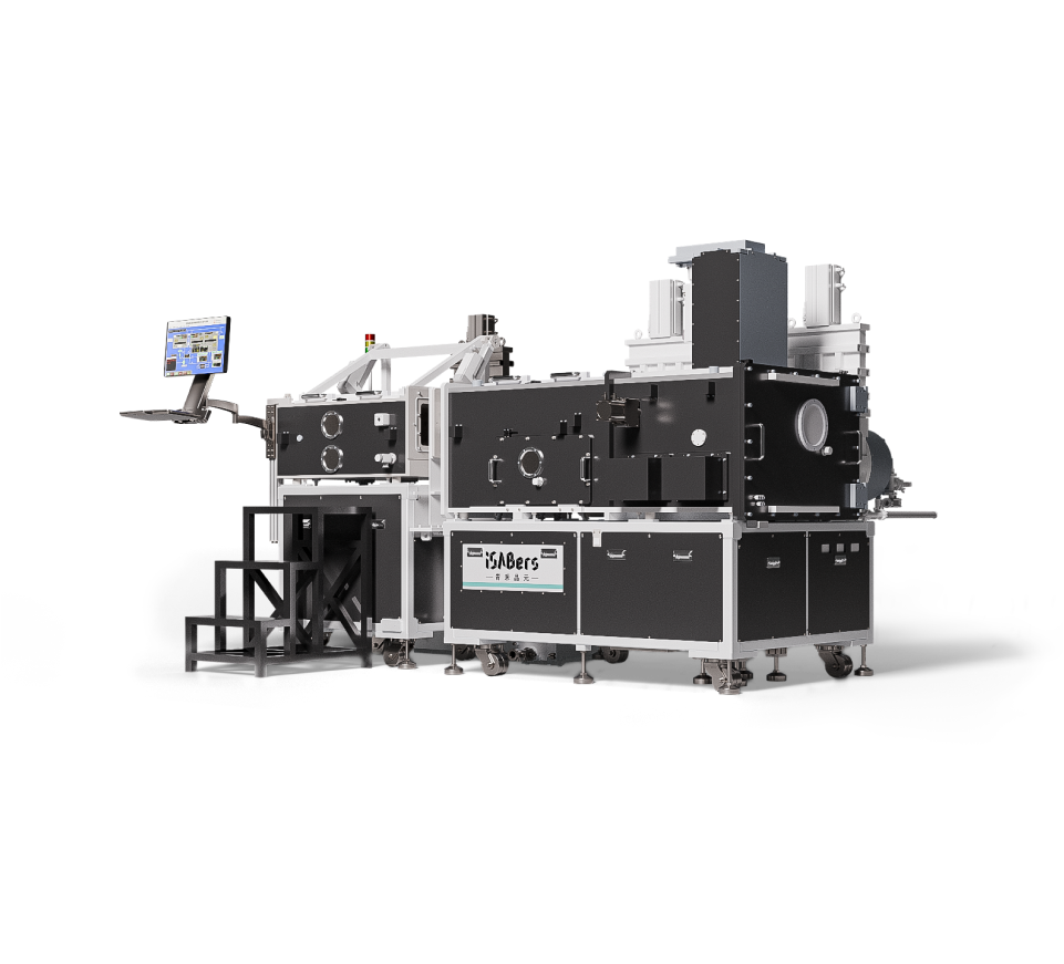
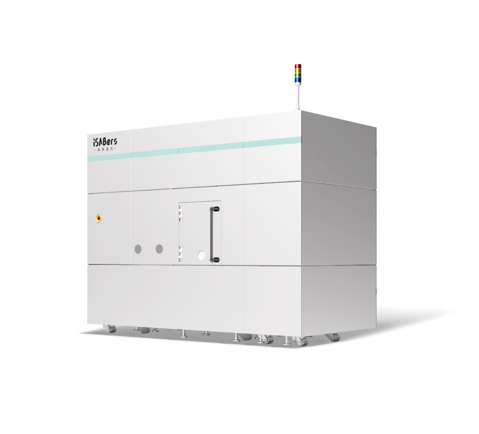
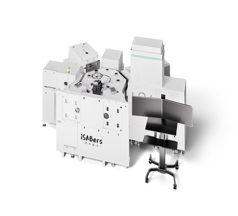
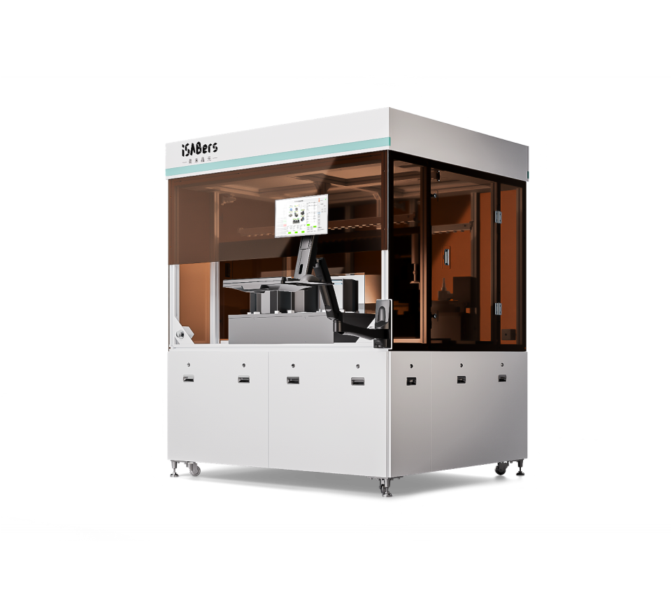
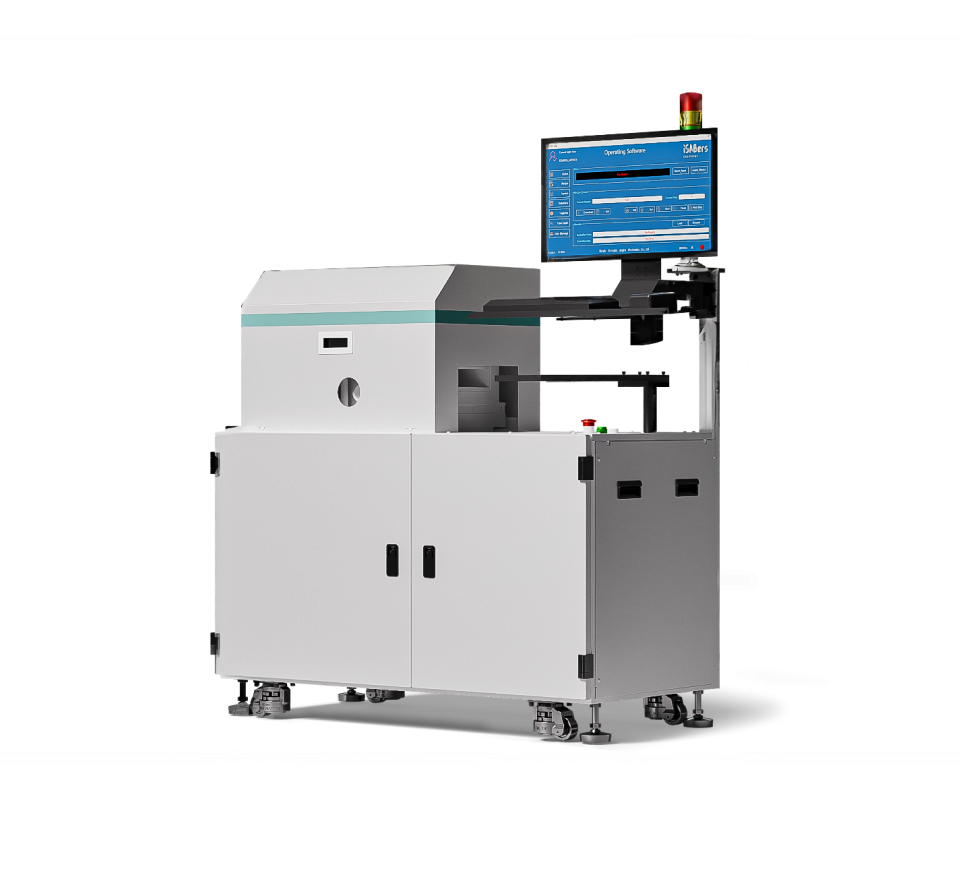
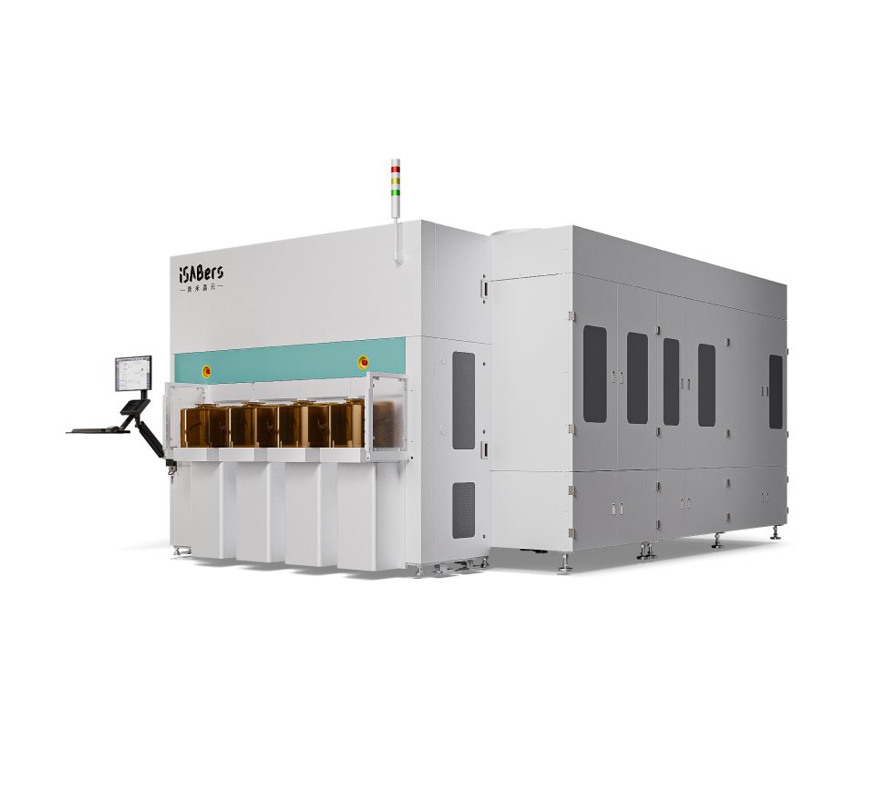
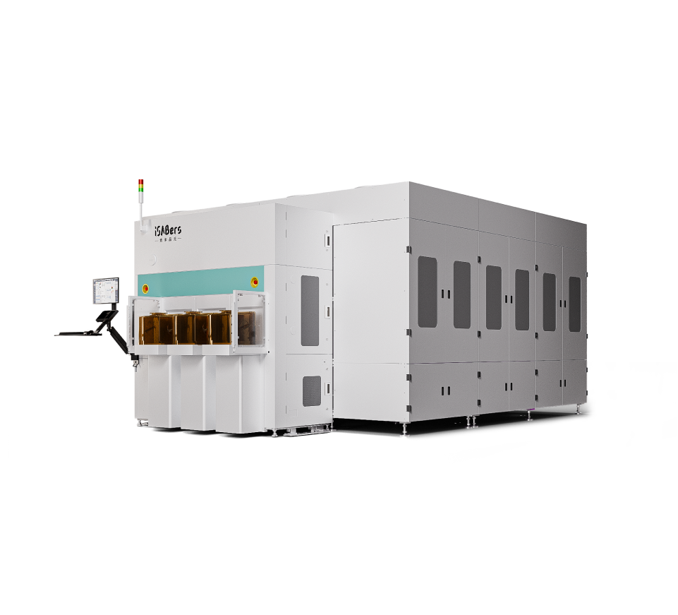
- Top-tier Equipment & Production Capacity
- Equipped with 100+ internationally advanced tools across 2,000㎡ total space, including 2,000㎡ of Class 10/100 cleanrooms. Annual capacity exceeds 60,000 wafers, supporting rapid prototyping and mid-volμme production.
-


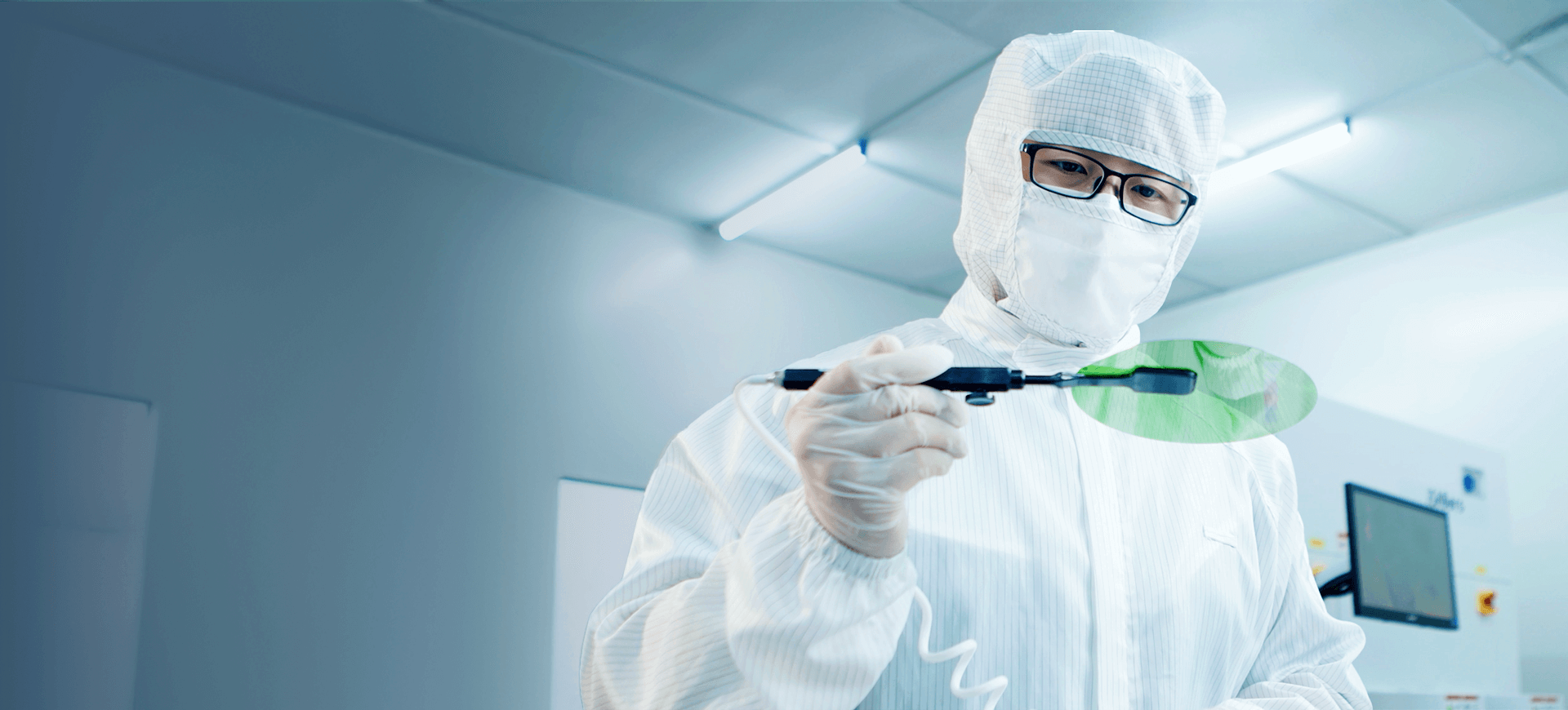
- Expert Team & Quality Assurance
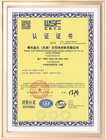
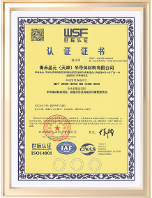
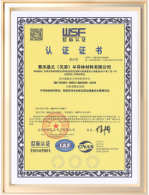
- 50+ senior engineers with core process teams exceeding 10 years' experience. Strict compliance with international quality standards including ISO 9001, IATF 16949, ISO 14001, and ISO 45001.
Accreditations
Application Cases