


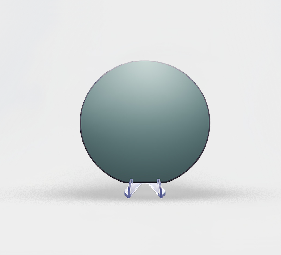
H-Cut SOI Substrate
- Items
- Specification
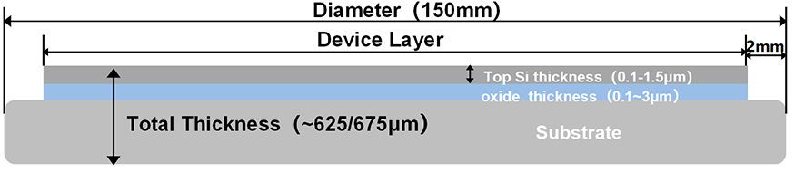
- Diameter
- 150±0.2mm
- SI Orientation
- <111>/<100>/<110>等
- Dopant Type
- P/N
- Device layer Si Thickness
- (0.1-1.5μm)±20nm
-
Edge Chip,Scratch,Crack
(visual inspection) - None
- Front roughness
-
Ra≤0.2nm
(5μm*5μm)
- BOX layer thickness
- 0.1~3μm
- Flat length
- 47.5/57.5±1.5mm
- TTV
- ≤5μm
- BOW
- -40~40μm
- Warp
- ≤50μm
- Total Thickness
- 625/675±25μm